 |
Zakładka z wyszukiwarką danych komponentów |
|
|
Zakładka z wyszukiwarką danych komponentów |
|
The question interval is too short.
Please try again in a few seconds.

Hello, Please ask a question about TS4851IJT Datasheet
# Example questions:
➢ How does increasing the gain (g) from the default setting to +12db (as seen in figure 8) affect the maximum achievable output power with a 4ω load?
➢ What is the difference in the specified test conditions (vcc, frequency, and load resistance) used for evaluating thd+n in figures 4, 5 and 8?
➢ In the psrr tests (referencing the data presented as graphs) what does the bandwidth (bw) of 125 khz signify, and how might a wider bandwidth affect the measured performance?
| Part No. | TS4851IJT |
| Manufacturer | STMICROELECTRONICS |
| Size | 1Mb |
| Pages | 28 pages |
| Description | MONO 1 W SPEAKER AND STEREO 160 mW HEADSET BTL DRIVERS WITH DIGITAL VOLUME CONTROL |




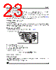


Okay, here's a summary of the information presented, focusing on the key electrical characteristics and what the provided tables/graphs illustrate. It's a bit messy since the data is presented as snippets of images, but I'll do my best to organize it.
Overall Context:
This document details the electrical characteristics of the TS4851 audio amplifier chip. It focuses on parameters like Total Harmonic Distortion + Noise (THD+N) as a function of output power, under various conditions.
Key Electrical Characteristics & Observations (from provided data):
️· THD+N vs. Output Power: The primary focus is on how THD+N changes with increasing output power. The graphs depict this relationship for different output modes and supply voltages (Vcc = 3V and 5V).
️· Output Modes: Several output modes are tested, including 1, 2, 3 and 7. The graphs indicate the THD+N performance varies with the output mode. Mode 3 has an additional gain setting (+12dB) which impacts the overall power/distortion characteristics.
️· Supply Voltage (Vcc): The performance is shown for both 3V and 5V supply voltages. Generally, higher Vcc results in higher maximum output power, but the effect on THD+N is more complex and depends on the specific output mode.
️· Load Resistance (RL): THD+N graphs are provided for various load resistances (4Ω, 8Ω, 16Ω, and 32Ω). The load impedance significantly impacts the THD+N curve.
️· Bandwidth (BW): The data indicates measurements were taken with a bandwidth limited to 125kHz.
️· Ambient Temperature (Tamb): Measurements were taken at 25°C.
Specific Data Points (from the provided snippets):
️· Figure 3 (Spkout THD+N vs. output power) – Output Modes 1 & 7: Shows THD+N vs. Output power for both 3V and 5V Vcc, using a 4Ω load, with BW < 125kHz at 25°C.
️· Figure 4 (Spkout THD+N vs. output power): Similar to Figure 3.
️· Figure 5 (Spkout THD+N vs. output power): Similar to Figures 3 and 4.
️· Figure 6 (HDout THD+N vs. output power – Output Mode 2): Shows THD+N vs. Output power for 3V and 5V with 32Ω loads.
️· Figure 7 (HDout THD+N vs. output power): Similar to Figure 6.
️· Figure 8 (Spkout THD+N vs. output power – Output Mode 3, G=+12dB): Shows THD+N vs. Output power with a 4Ω load.
Trends & General Observations (from limited data):
️· Increasing Output Power, Increasing Distortion: As output power increases, THD+N generally increases. This is typical for audio amplifiers.
️· Supply Voltage Effects: Higher Vcc generally allows for more output power before significant distortion occurs.
️· Load Resistance Effects: Lower load resistance (e.g., 4Ω) often leads to higher distortion levels than higher load resistances.
Important Note:
The provided data is fragmented. A complete datasheet would provide more comprehensive information, including absolute maximum ratings, minimum/typical/maximum values for all parameters, and detailed test conditions.
If you have specific questions about a particular output mode, load resistance, or supply voltage, I can try to extract information from the provided images.
Overall Context:
This document details the electrical characteristics of the TS4851 audio amplifier chip. It focuses on parameters like Total Harmonic Distortion + Noise (THD+N) as a function of output power, under various conditions.
Key Electrical Characteristics & Observations (from provided data):
️· THD+N vs. Output Power: The primary focus is on how THD+N changes with increasing output power. The graphs depict this relationship for different output modes and supply voltages (Vcc = 3V and 5V).
️· Output Modes: Several output modes are tested, including 1, 2, 3 and 7. The graphs indicate the THD+N performance varies with the output mode. Mode 3 has an additional gain setting (+12dB) which impacts the overall power/distortion characteristics.
️· Supply Voltage (Vcc): The performance is shown for both 3V and 5V supply voltages. Generally, higher Vcc results in higher maximum output power, but the effect on THD+N is more complex and depends on the specific output mode.
️· Load Resistance (RL): THD+N graphs are provided for various load resistances (4Ω, 8Ω, 16Ω, and 32Ω). The load impedance significantly impacts the THD+N curve.
️· Bandwidth (BW): The data indicates measurements were taken with a bandwidth limited to 125kHz.
️· Ambient Temperature (Tamb): Measurements were taken at 25°C.
Specific Data Points (from the provided snippets):
️· Figure 3 (Spkout THD+N vs. output power) – Output Modes 1 & 7: Shows THD+N vs. Output power for both 3V and 5V Vcc, using a 4Ω load, with BW < 125kHz at 25°C.
️· Figure 4 (Spkout THD+N vs. output power): Similar to Figure 3.
️· Figure 5 (Spkout THD+N vs. output power): Similar to Figures 3 and 4.
️· Figure 6 (HDout THD+N vs. output power – Output Mode 2): Shows THD+N vs. Output power for 3V and 5V with 32Ω loads.
️· Figure 7 (HDout THD+N vs. output power): Similar to Figure 6.
️· Figure 8 (Spkout THD+N vs. output power – Output Mode 3, G=+12dB): Shows THD+N vs. Output power with a 4Ω load.
Trends & General Observations (from limited data):
️· Increasing Output Power, Increasing Distortion: As output power increases, THD+N generally increases. This is typical for audio amplifiers.
️· Supply Voltage Effects: Higher Vcc generally allows for more output power before significant distortion occurs.
️· Load Resistance Effects: Lower load resistance (e.g., 4Ω) often leads to higher distortion levels than higher load resistances.
Important Note:
The provided data is fragmented. A complete datasheet would provide more comprehensive information, including absolute maximum ratings, minimum/typical/maximum values for all parameters, and detailed test conditions.
| Part No. | TS4851IJT |
| Manufacturer | STMICROELECTRONICS |
| Size | 1Mb |
| Pages | 28 pages |
| Description | MONO 1 W SPEAKER AND STEREO 160 mW HEADSET BTL DRIVERS WITH DIGITAL VOLUME CONTROL |
| Czy Alldatasheet okazała się pomocna? [ DONATE ] |
O Alldatasheet | Reklama | Kontakt | Polityka prywatności | Link do karty katalogowej | Linki | Lista producentów All Rights Reserved©Alldatasheet.com |
| Russian : Alldatasheetru.com | Korean : Alldatasheet.co.kr | Spanish : Alldatasheet.es | French : Alldatasheet.fr | Italian : Alldatasheetit.com Portuguese : Alldatasheetpt.com | Polish : Alldatasheet.pl | Vietnamese : Alldatasheet.vn Indian : Alldatasheet.in | Mexican : Alldatasheet.com.mx | British : Alldatasheet.co.uk | New Zealand : Alldatasheet.co.nz |
|
Family Site : ic2ic.com |
icmetro.com |
 Polish ▼
  English
 Chinese
 German
 Japanese
 Russian
 Korean
 Spanish
 French
 Italian
 Portuguese
 Vietnamese
 Indian
 Mexican
 British
 New Zealand