 |
Zakładka z wyszukiwarką danych komponentów |
|
|
Zakładka z wyszukiwarką danych komponentów |
|
The question interval is too short.
Please try again in a few seconds.

Hello, Please ask a question about AD5544ACPZ-1-R2 Datasheet
# Example questions:
➢ What are the absolute maximum ratings for vdd to gnd and vrefx to gnd?
➢ What is the typical thermal resistance (θja) for both the 28-lead ssop and 32-lead lfcsp packages?
➢ What is the typical maximum junction temperature (tj max) for the ad5544/ad5554, and what are the operating and storage temperature ranges?
| Part No. | AD5544ACPZ-1-R2 |
| Manufacturer | AD |
| Size | 735 Kbytes |
| Pages | 24 pages |
| Description | Quad, Current-Output, Serial-Input 16-/14-Bit DACs |


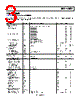


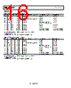


1. General Information & Overview:
️· Devices: This data sheet covers the AD5544 and AD5554. They are likely similar devices (the data is often duplicated across them) but may have minor differences (like some timing parameters - check the full datasheets).
️· Function: They are Digital-to-Analog Converters (DACs). This means they convert digital signals (binary numbers) into analog voltage signals.
️· Applications: (Not explicitly stated in these excerpts, but implied) Precision voltage output, data acquisition systems, industrial control, etc.
️· ESD Caution: Important reminder to handle the devices with Electrostatic Discharge (ESD) precautions.
2. Electrical Characteristics (Key Highlights)
These are just a selection of values - a complete list is in the full datasheet.
️· Absolute Maximum Ratings: These are stress limits. Exceeding them *can* damage the device. Important values include:
- Supply Voltages (VDD, VSS, VREFx): Ranges with limits on both positive and negative values.
- Input/Output Voltages: Limits on voltage levels.
- Input Current: Maximum current allowed to flow into pins.
- Power Dissipation/Thermal Resistance: Maximum heat the device can dissipate. Temperature limits are also defined.
️· Operating Characteristics (from Table 4 - not included in these excerpts): These describe how the DACs perform under typical operating conditions.
️· Logic Input/Output:
- Logic Input Low/High Voltages (VIL/VIH): Defines the voltage levels that are interpreted as logic 0 and 1.
- Input Leakage Current (IIL): Small current that flows into the input pins.
- Logic Output Low/High Voltages (VOL/VOH): Voltages at the logic output pins when in the low/high state.
️· Timing Parameters: (Refer to the Timing Diagrams and Table 2): These are very important for synchronization and data transfer. They specify delays and setup/hold times for signals like clock, data, and chip select. Some key values:
- Clock Width High (tCH) / Clock Width Low (tCL) : Defines the duration of high and low clock pulses.
- CS to Clock Setup Time (tCSS): How much time before the clock signal that the CS signal needs to be asserted.
- Clock to SDO Propagation Delay (tPD): The time it takes for data to propagate from the clock signal to the SDO output.
3. Physical Characteristics & Package Information:
️· Package Options: Available in SSOP (Small Outline Package) and LFCSP (Lead Frame Chip Scale Package)
️· Thermal Resistance: Different values for each package.
4. Key Diagrams & Figures:
️· Timing Diagrams: (Figure 1 and Figure 2) - Essential for understanding the sequence and timing of signals during operation. These show how the DAC responds to signals like clock, data, and chip select.
1. General Information & Overview:
️· Devices: This data sheet covers the AD5544 and AD5554. They are likely similar devices (the data is often duplicated across them) but may have minor differences (like some timing parameters - check the full datasheets).
️· Function: They are Digital-to-Analog Converters (DACs). This means they convert digital signals (binary numbers) into analog voltage signals.
️· Applications: (Not explicitly stated in these excerpts, but implied) Precision voltage output, data acquisition systems, industrial control, etc.
️· ESD Caution: Important reminder to handle the devices with Electrostatic Discharge (ESD) precautions.
2. Electrical Characteristics (Key Highlights)
These are just a selection of values - a complete list is in the full datasheet.
️· Absolute Maximum Ratings: These are stress limits. Exceeding them *can* damage the device. Important values include:
- Supply Voltages (VDD, VSS, VREFx): Ranges with limits on both positive and negative values.
- Input/Output Voltages: Limits on voltage levels.
- Input Current: Maximum current allowed to flow into pins.
- Power Dissipation/Thermal Resistance: Maximum heat the device can dissipate. Temperature limits are also defined.
️· Operating Characteristics (from Table 4 - not included in these excerpts): These describe how the DACs perform under typical operating conditions.
️· Logic Input/Output:
- Logic Input Low/High Voltages (VIL/VIH): Defines the voltage levels that are interpreted as logic 0 and 1.
- Input Leakage Current (IIL): Small current that flows into the input pins.
- Logic Output Low/High Voltages (VOL/VOH): Voltages at the logic output pins when in the low/high state.
️· Timing Parameters: (Refer to the Timing Diagrams and Table 2): These are very important for synchronization and data transfer. They specify delays and setup/hold times for signals like clock, data, and chip select. Some key values:
- Clock Width High (tCH) / Clock Width Low (tCL) : Defines the duration of high and low clock pulses.
- CS to Clock Setup Time (tCSS): How much time before the clock signal that the CS signal needs to be asserted.
- Clock to SDO Propagation Delay (tPD): The time it takes for data to propagate from the clock signal to the SDO output.
3. Physical Characteristics & Package Information:
️· Package Options: Available in SSOP (Small Outline Package) and LFCSP (Lead Frame Chip Scale Package)
️· Thermal Resistance: Different values for each package.
4. Key Diagrams & Figures:
️· Timing Diagrams: (Figure 1 and Figure 2) - Essential for understanding the sequence and timing of signals during operation. These show how the DAC responds to signals like clock, data, and chip select.
| Part No. | AD5544ACPZ-1-R2 |
| Manufacturer | AD |
| Size | 735 Kbytes |
| Pages | 24 pages |
| Description | Quad, Current-Output, Serial-Input 16-/14-Bit DACs |
| Czy Alldatasheet okazała się pomocna? [ DONATE ] |
O Alldatasheet | Reklama | Kontakt | Polityka prywatności | Link do karty katalogowej | Linki | Lista producentów All Rights Reserved©Alldatasheet.com |
| Russian : Alldatasheetru.com | Korean : Alldatasheet.co.kr | Spanish : Alldatasheet.es | French : Alldatasheet.fr | Italian : Alldatasheetit.com Portuguese : Alldatasheetpt.com | Polish : Alldatasheet.pl | Vietnamese : Alldatasheet.vn Indian : Alldatasheet.in | Mexican : Alldatasheet.com.mx | British : Alldatasheet.co.uk | New Zealand : Alldatasheet.co.nz |
|
Family Site : ic2ic.com |
icmetro.com |
 Polish ▼
  English
 Chinese
 German
 Japanese
 Russian
 Korean
 Spanish
 French
 Italian
 Portuguese
 Vietnamese
 Indian
 Mexican
 British
 New Zealand