 |
Zakładka z wyszukiwarką danych komponentów |
|
|
Zakładka z wyszukiwarką danych komponentów |
|
The question interval is too short.
Please try again in a few seconds.

Hello, Please ask a question about MP2012DQ Datasheet
# Example questions:
➢ What is the maximum allowable lead coplanarity for the qfn6 package?
➢ What is the recommended land pattern variation referenced in the package information section?
➢ What jedec reference is cited for the qfn6 package variation?
| Part No. | MP2012DQ |
| Manufacturer | MPS |
| Size | 328 Kbytes |
| Pages | 10 pages |
| Description | Low Voltage, 2.7-6V Input,1.5A, 1.2MHz Synchronous Step-Down Converter |

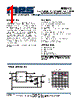


1. Overview:
️· What is it? The MP2012 is a synchronous buck regulator, designed to efficiently convert a voltage source down to a lower voltage. It's targeted at applications requiring a small footprint and efficient power delivery.
️· Key Features: Synchronous rectification (uses a MOSFET instead of a diode, boosting efficiency), small size (QFN package), good transient response, and adjustable switching frequency.
2. Electrical Characteristics & Operation:
️· Input Voltage Range: Not explicitly stated in the provided text, but would be critical.
️· Output Voltage: Adjustable, likely through external resistors (details not fully detailed in this excerpt).
️· Switching Frequency: Adjustable.
️· Efficiency: High efficiency due to synchronous rectification.
️· Operation: It operates by rapidly switching the input voltage on and off, storing energy in an inductor and transferring it to the output capacitor. The synchronous MOSFET replaces the diode in a traditional buck converter, reducing losses.
3. Applications:
️· Portable electronics (phones, tablets)
️· Battery-powered devices
️· Point-of-load regulation
️· Any application needing efficient voltage conversion in a small space.
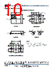
4. Package Information:
️· Package Type: QFN6 (6-pin, 3mm x 3mm) – very small surface-mount package
️· Pad Layout: Important for thermal management and proper device operation. The datasheet includes layout recommendations.
️· Pinout: (Refer to the datasheet for a pin diagram, but this would include VIN, GND, SW, FB, EN and potentially an exposed pad for thermal dissipation).
5. Design Considerations & Layout Recommendations:
️· PCB Layout: Extremely important for performance. Recommendations include:
- Short, wide traces for high-current paths (VIN, GND, SW).
- Close placement of input capacitors.
- Placement of feedback resistors near the FB pin.
- Avoid ground loops.
️· Thermal Management: The small package size means that heat dissipation is a concern. Proper PCB layout and potentially heat spreading techniques may be necessary.
6. Important Notes:
️· Design Responsibilities: MPS does not assume responsibility for third-party intellectual property rights infringements or legal liabilities.
️· Datasheet Updates: The information is subject to change without notice, so always refer to the latest version of the datasheet.
1. Overview:
️· What is it? The MP2012 is a synchronous buck regulator, designed to efficiently convert a voltage source down to a lower voltage. It's targeted at applications requiring a small footprint and efficient power delivery.
️· Key Features: Synchronous rectification (uses a MOSFET instead of a diode, boosting efficiency), small size (QFN package), good transient response, and adjustable switching frequency.
2. Electrical Characteristics & Operation:
️· Input Voltage Range: Not explicitly stated in the provided text, but would be critical.
️· Output Voltage: Adjustable, likely through external resistors (details not fully detailed in this excerpt).
️· Switching Frequency: Adjustable.
️· Efficiency: High efficiency due to synchronous rectification.
️· Operation: It operates by rapidly switching the input voltage on and off, storing energy in an inductor and transferring it to the output capacitor. The synchronous MOSFET replaces the diode in a traditional buck converter, reducing losses.
3. Applications:
️· Portable electronics (phones, tablets)
️· Battery-powered devices
️· Point-of-load regulation
️· Any application needing efficient voltage conversion in a small space.
4. Package Information:
️· Package Type: QFN6 (6-pin, 3mm x 3mm) – very small surface-mount package
️· Pad Layout: Important for thermal management and proper device operation. The datasheet includes layout recommendations.
️· Pinout: (Refer to the datasheet for a pin diagram, but this would include VIN, GND, SW, FB, EN and potentially an exposed pad for thermal dissipation).
5. Design Considerations & Layout Recommendations:
️· PCB Layout: Extremely important for performance. Recommendations include:
- Short, wide traces for high-current paths (VIN, GND, SW).
- Close placement of input capacitors.
- Placement of feedback resistors near the FB pin.
- Avoid ground loops.
️· Thermal Management: The small package size means that heat dissipation is a concern. Proper PCB layout and potentially heat spreading techniques may be necessary.
6. Important Notes:
️· Design Responsibilities: MPS does not assume responsibility for third-party intellectual property rights infringements or legal liabilities.
️· Datasheet Updates: The information is subject to change without notice, so always refer to the latest version of the datasheet.
| Part No. | MP2012DQ |
| Manufacturer | MPS |
| Size | 328 Kbytes |
| Pages | 10 pages |
| Description | Low Voltage, 2.7-6V Input,1.5A, 1.2MHz Synchronous Step-Down Converter |
| Czy Alldatasheet okazała się pomocna? [ DONATE ] |
O Alldatasheet | Reklama | Kontakt | Polityka prywatności | Link do karty katalogowej | Linki | Lista producentów All Rights Reserved©Alldatasheet.com |
| Russian : Alldatasheetru.com | Korean : Alldatasheet.co.kr | Spanish : Alldatasheet.es | French : Alldatasheet.fr | Italian : Alldatasheetit.com Portuguese : Alldatasheetpt.com | Polish : Alldatasheet.pl | Vietnamese : Alldatasheet.vn Indian : Alldatasheet.in | Mexican : Alldatasheet.com.mx | British : Alldatasheet.co.uk | New Zealand : Alldatasheet.co.nz |
|
Family Site : ic2ic.com |
icmetro.com |
 Polish ▼
  English
 Chinese
 German
 Japanese
 Russian
 Korean
 Spanish
 French
 Italian
 Portuguese
 Vietnamese
 Indian
 Mexican
 British
 New Zealand