 |
Zakładka z wyszukiwarką danych komponentów |
|
|
Zakładka z wyszukiwarką danych komponentów |
|
The question interval is too short.
Please try again in a few seconds.

Hello, Please ask a question about LTC1690 Datasheet
# Example questions:
➢ What parameter is represented by the graphs labeled '1690 g01', '1690 g02', and '1690 g03'?
➢ What is the range of common-mode input voltage (vcm) for which receiver characteristics are specified?
➢ What is the typical supply voltage (vcc) used in the performance characteristics described in the document?
| Part No. | LTC1690 |
| Manufacturer | LINER |
| Size | 221 Kbytes |
| Pages | 12 pages |
| Description | Differential Driver and Receiver Pair with Fail-Safe Receiver Output |




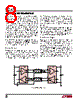


1. Overall Purpose:
️· Data Sheet Excerpt: This isn't the whole document, but a section focused on input threshold voltages and hysteresis of a receiver circuit.
️· Logic Family Device: It's for a logic device within the 54/74 series (or similar) as indicated by the mention of "54/74". These are common TTL (Transistor-Transistor Logic) chips.
️· Focus on Input Levels: The core information concerns the voltage levels at which the receiver changes state (from low to high, or high to low).
2. Key Terms and Concepts
️· VCM (Common-Mode Input Voltage): This is the voltage applied to both inputs of the comparator or receiver. The data is presented for several values:
- 12V: A high common-mode voltage.
- 0V: A ground reference.
- -7V: A negative voltage reference.
️· Input Threshold Voltage (VTH): This is the voltage at which the receiver transitions between a low and high output state. There's a distinction between Upper Threshold Voltage (VTH – High) and Lower Threshold Voltage (VTH – Low).
️· Hysteresis: This is crucial. It means the threshold voltage *changes* depending on whether the input was previously high or low. A positive hysteresis value means that the voltage needed to switch from low to high is higher than the voltage required to switch from high to low. This prevents unwanted oscillations (chattering) when the input signal is near a threshold.
️· Temperature: The values are given across a temperature range (likely -40°C to +85°C, typical for industrial electronics, though the specific values would depend on the device's datasheet).
3. Data Presentation
️· Graphs: The excerpt describes multiple graphs (labeled "1690 G01", "1690 G02", "1690 G03"), each representing:
- G01: Input Threshold Voltage (Output High) vs. Temperature for various VCM values.
- G02: Input Threshold Voltage (Output Low) vs. Temperature for various VCM values.
- G03: Hysteresis vs. Temperature for various VCM values.
4. What can you learn from this data?
️· Input Level Design: You can determine what voltage ranges you need to use for your input signals to ensure reliable logic operation.
️· Noise Immunity: The hysteresis helps to filter out noise and spurious signals.
️· Temperature Effects: Understand how temperature changes will affect the logic levels. If you're operating in a wide temperature range, you need to account for these shifts.
️· Debugging: If you've got logic problems, these tables help you narrow down the cause.
Limitations from just this excerpt:
️· Device Identification: We don't know *which* specific chip this refers to. The datasheet would have a part number.
️· Full Specs: This is only part of a datasheet. Other specifications like power supply requirements, propagation delays, and output drive capability aren't shown.
️· Graph Details: The exact scales and resolution of the graphs aren't stated, so interpretation would require a visual representation.
1. Overall Purpose:
️· Data Sheet Excerpt: This isn't the whole document, but a section focused on input threshold voltages and hysteresis of a receiver circuit.
️· Logic Family Device: It's for a logic device within the 54/74 series (or similar) as indicated by the mention of "54/74". These are common TTL (Transistor-Transistor Logic) chips.
️· Focus on Input Levels: The core information concerns the voltage levels at which the receiver changes state (from low to high, or high to low).
2. Key Terms and Concepts
️· VCM (Common-Mode Input Voltage): This is the voltage applied to both inputs of the comparator or receiver. The data is presented for several values:
- 12V: A high common-mode voltage.
- 0V: A ground reference.
- -7V: A negative voltage reference.
️· Input Threshold Voltage (VTH): This is the voltage at which the receiver transitions between a low and high output state. There's a distinction between Upper Threshold Voltage (VTH – High) and Lower Threshold Voltage (VTH – Low).
️· Hysteresis: This is crucial. It means the threshold voltage *changes* depending on whether the input was previously high or low. A positive hysteresis value means that the voltage needed to switch from low to high is higher than the voltage required to switch from high to low. This prevents unwanted oscillations (chattering) when the input signal is near a threshold.
️· Temperature: The values are given across a temperature range (likely -40°C to +85°C, typical for industrial electronics, though the specific values would depend on the device's datasheet).
3. Data Presentation
️· Graphs: The excerpt describes multiple graphs (labeled "1690 G01", "1690 G02", "1690 G03"), each representing:
- G01: Input Threshold Voltage (Output High) vs. Temperature for various VCM values.
- G02: Input Threshold Voltage (Output Low) vs. Temperature for various VCM values.
- G03: Hysteresis vs. Temperature for various VCM values.
4. What can you learn from this data?
️· Input Level Design: You can determine what voltage ranges you need to use for your input signals to ensure reliable logic operation.
️· Noise Immunity: The hysteresis helps to filter out noise and spurious signals.
️· Temperature Effects: Understand how temperature changes will affect the logic levels. If you're operating in a wide temperature range, you need to account for these shifts.
️· Debugging: If you've got logic problems, these tables help you narrow down the cause.
Limitations from just this excerpt:
️· Device Identification: We don't know *which* specific chip this refers to. The datasheet would have a part number.
️· Full Specs: This is only part of a datasheet. Other specifications like power supply requirements, propagation delays, and output drive capability aren't shown.
️· Graph Details: The exact scales and resolution of the graphs aren't stated, so interpretation would require a visual representation.
| Part No. | LTC1690 |
| Manufacturer | LINER |
| Size | 221 Kbytes |
| Pages | 12 pages |
| Description | Differential Driver and Receiver Pair with Fail-Safe Receiver Output |
| Czy Alldatasheet okazała się pomocna? [ DONATE ] |
O Alldatasheet | Reklama | Kontakt | Polityka prywatności | Link do karty katalogowej | Linki | Lista producentów All Rights Reserved©Alldatasheet.com |
| Russian : Alldatasheetru.com | Korean : Alldatasheet.co.kr | Spanish : Alldatasheet.es | French : Alldatasheet.fr | Italian : Alldatasheetit.com Portuguese : Alldatasheetpt.com | Polish : Alldatasheet.pl | Vietnamese : Alldatasheet.vn Indian : Alldatasheet.in | Mexican : Alldatasheet.com.mx | British : Alldatasheet.co.uk | New Zealand : Alldatasheet.co.nz |
|
Family Site : ic2ic.com |
icmetro.com |
 Polish ▼
  English
 Chinese
 German
 Japanese
 Russian
 Korean
 Spanish
 French
 Italian
 Portuguese
 Vietnamese
 Indian
 Mexican
 British
 New Zealand