 |
Zakładka z wyszukiwarką danych komponentów |
|
|
Zakładka z wyszukiwarką danych komponentów |
|
The question interval is too short.
Please try again in a few seconds.

Hello, Please ask a question about BD242 Datasheet
# Example questions:
➢ What are the maximum collector-emitter voltage (vce) and collector current (ic) ratings for the bd242c transistor?
➢ What are the minimum and maximum dimensions for dimension 'f' in the to-220 package, as specified in the mechanical data table?
➢ What is the typical hfe (dc current gain) of the bd242b transistor when vce = -4v and ic = -1a?
| Part No. | BD242 |
| Manufacturer | COMSET |
| Size | 104 Kbytes |
| Pages | 3 pages |
| Description | MEDIUM POWER LINEAR AND SWITCHING APPLICATIONS |

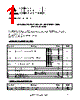
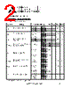
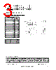

Okay, here's a comprehensive summary of the provided datasheet for the BD242 (and its variants A, B, and C) transistors:
1. General Description:
️· The BD242, BD242A, BD242B, and BD242C are PNP silicon power transistors. They are designed for general purpose amplification and switching applications. The key difference between the variants (A, B, C) appears to be variations in their electrical characteristics, especially hFE (DC Current Gain).
2. Key Electrical Characteristics (Highlights - values vary by variant, refer to datasheet for specifics):
️· VCEO (Collector-Emitter Voltage): Ranges from 40V to 100V depending on the variant.
️· IC (Collector Current): Maximum continuous collector current of 3A.
️· hFE (DC Current Gain): This is a key differentiating factor between the variants:
- BD242: Ranges considerably, approximately 25-350
- BD242A, B, C: Similar ranges, but with potentially slightly different specific values. Refer to the tables for exact values.
️· VCE(sat) (Collector-Emitter Saturation Voltage): Around 1.2V (typical).
️· VBE(on) (Base-Emitter Voltage): Around 1.8V (typical).
️· f(hFE) (Transition Frequency): The BD242 has a transition frequency in the MHz range.
️· Conditions for Pulsed Tests: Important to note that some specifications (like VCE(sat) and hFE) are measured under pulsed conditions (Pulse Width ≈ 300 µs, Duty Cycle ≤ 2.0%). This means the values might be slightly different under continuous operation.
3. Mechanical Details:
️· Package: TO-220.
️· Pinout:
- Pin 1: Base
- Pin 2: Collector
- Pin 3: Emitter
4. Important Notes & Disclaimers:
️· Variant Differences: The variants (A, B, and C) have subtly different electrical characteristics, particularly hFE. Always consult the specific table for the variant you are using.
️· Pulsed Operation: Certain measurements are done under pulsed conditions. Consider this when designing your circuit.
️· Standard Disclaimer: The manufacturer disclaims responsibility for consequences of using the information. They also state that the transistors are not authorized for life support systems.
To get more specific values, always refer to the provided datasheet tables.
1. General Description:
️· The BD242, BD242A, BD242B, and BD242C are PNP silicon power transistors. They are designed for general purpose amplification and switching applications. The key difference between the variants (A, B, C) appears to be variations in their electrical characteristics, especially hFE (DC Current Gain).
2. Key Electrical Characteristics (Highlights - values vary by variant, refer to datasheet for specifics):
️· VCEO (Collector-Emitter Voltage): Ranges from 40V to 100V depending on the variant.
️· IC (Collector Current): Maximum continuous collector current of 3A.
️· hFE (DC Current Gain): This is a key differentiating factor between the variants:
- BD242: Ranges considerably, approximately 25-350
- BD242A, B, C: Similar ranges, but with potentially slightly different specific values. Refer to the tables for exact values.
️· VCE(sat) (Collector-Emitter Saturation Voltage): Around 1.2V (typical).
️· VBE(on) (Base-Emitter Voltage): Around 1.8V (typical).
️· f(hFE) (Transition Frequency): The BD242 has a transition frequency in the MHz range.
️· Conditions for Pulsed Tests: Important to note that some specifications (like VCE(sat) and hFE) are measured under pulsed conditions (Pulse Width ≈ 300 µs, Duty Cycle ≤ 2.0%). This means the values might be slightly different under continuous operation.
3. Mechanical Details:
️· Package: TO-220.
️· Pinout:
- Pin 1: Base
- Pin 2: Collector
- Pin 3: Emitter
4. Important Notes & Disclaimers:
️· Variant Differences: The variants (A, B, and C) have subtly different electrical characteristics, particularly hFE. Always consult the specific table for the variant you are using.
️· Pulsed Operation: Certain measurements are done under pulsed conditions. Consider this when designing your circuit.
️· Standard Disclaimer: The manufacturer disclaims responsibility for consequences of using the information. They also state that the transistors are not authorized for life support systems.
| Part No. | BD242 |
| Manufacturer | COMSET |
| Size | 104 Kbytes |
| Pages | 3 pages |
| Description | MEDIUM POWER LINEAR AND SWITCHING APPLICATIONS |
| Czy Alldatasheet okazała się pomocna? [ DONATE ] |
O Alldatasheet | Reklama | Kontakt | Polityka prywatności | Link do karty katalogowej | Linki | Lista producentów All Rights Reserved©Alldatasheet.com |
| Russian : Alldatasheetru.com | Korean : Alldatasheet.co.kr | Spanish : Alldatasheet.es | French : Alldatasheet.fr | Italian : Alldatasheetit.com Portuguese : Alldatasheetpt.com | Polish : Alldatasheet.pl | Vietnamese : Alldatasheet.vn Indian : Alldatasheet.in | Mexican : Alldatasheet.com.mx | British : Alldatasheet.co.uk | New Zealand : Alldatasheet.co.nz |
|
Family Site : ic2ic.com |
icmetro.com |
 Polish ▼
  English
 Chinese
 German
 Japanese
 Russian
 Korean
 Spanish
 French
 Italian
 Portuguese
 Vietnamese
 Indian
 Mexican
 British
 New Zealand