|
Zakładka z wyszukiwarką danych komponentów |
|
|
Zakładka z wyszukiwarką danych komponentów |
|
AD797 Arkusz danych(PDF) 13 Page - Analog Devices |
|
|
|||||||||||||||||||||||||||||
AD797 Arkusz danych(HTML) 13 Page - Analog Devices |
|
|
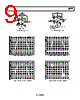
13 / 20 page  AD797 Rev. F | Page 13 of 20 USE SHORT LEAD LENGTHS (<5mm) KELVIN RETURN LOAD CURRENT OR 0.1µF VS VS 4.7µF USE SHORT LEAD LENGTHS (<5mm) KELVIN RETURN LOAD CURRENT 0.1µF 4.7µF TO 22.0µF 1.1Ω TO 4.7Ω Figure 35. Recommended Power Supply Bypassing THE NONINVERTING CONFIGURATION Ultralow noise requires very low values of the internal parasitic resistance (rBB) for the input transistors (≈6 Ω). This implies very little damping of input and output reactive interactions. With the AD797, additional input series damping is required for stability with direct output to input feedback. A 100 Ω resistor (R1) in the inverting input (Figure 36) is sufficient; the 100 Ω balancing resistor (R2) is recommended but is not required for stability. The noise penalty is minimal (eNtotal ≈ 2.1 nV/√Hz), which is usually insignificant. 7 4 3 R2 100Ω R1 100Ω * * VOUT VIN +VS –VS AD797 RL 600Ω 6 2 *USE THE POWER SUPPLY BYPASSING SHOWN IN FIGURE 35. Figure 36. Voltage Follower Connection Best response flatness is obtained with the addition of a small capacitor (CL < 33 pF) in parallel with the 100 Ω resistor (Figure 37). The input source resistance and capacitance also affect the response slightly, and experimentation may be necessary for best results. 7 * *USE THE POWER SUPPLY BYPASSING SHOWN IN FIGURE 35. * VOUT VIN +VS –VS AD797 CL 6 2 RS CS 3 4 600Ω 100Ω Figure 37. Alternative Voltage Follower Connection Low noise preamplification is usually performed in the non- inverting mode (Figure 38). For lowest noise, the equivalent resistance of the feedback network should be as low as possible. The 30 mA minimum drive current of the AD797 makes it easier to achieve this. The feedback resistors can be made as low as possible, with consideration to load drive and power consumption. 7 * * VOUT VIN +VS –VS AD797 RL CL R2 R1 6 2 3 4 *USE THE POWER SUPPLY BYPASSING SHOWN IN FIGURE 35. Figure 38. Low Noise Preamplifier Table 4 provides some representative values for the AD797 when used as a low noise follower. Operation on 5 V supplies allows the use of a 100 Ω or less feedback network (R1 + R2). Because the AD797 shows no unusual behavior when operating near its maximum rated current, it is suitable for driving the AD600/AD602 (see Figure 50) while preserving low noise performance. Optimum flatness and stability at noise gains >1 sometimes require a small capacitor (CL) connected across the feedback resistor (R1 of Figure 38). Table 4 includes recommended values of CL for several gains. In general, when R2 is greater than 100 Ω and CL is greater than 33 pF, a 100 Ω resistor should be placed in series with CL. Source resistance matching is assumed, and the AD797 should not be operated with unbalanced source resistance >200 kΩ/G. Table 4. Values for Follower with Gain Circuit Gain R1 R2 CL Noise (Excluding RS) 2 1 kΩ 1 kΩ ≈20 pF 3.0 nV/√Hz 2 300 Ω 300 Ω ≈10 pF 1.8 nV/√Hz 10 33.2 Ω 300 Ω ≈5 pF 1.2 nV/√Hz 20 16.5 Ω 316 Ω 1.0 nV/√Hz >35 10 Ω (G − 1) × 10 Ω 0.98 nV/√Hz The I-to-V converter is a special case of the follower configu- ration. When the AD797 is used in an I-to-V converter, for example as a DAC buffer, the circuit shown in Figure 39 should be used. The value of CL depends on the DAC, and if CL is greater than 33 pF, a 100 Ω series resistor is required. A bypassed balancing resistor (RS and CS) can be included to minimize dc errors. |
|
|
Link URL |
| Czy Alldatasheet okazała się pomocna? [ DONATE ] |
O Alldatasheet | Reklama | Kontakt | Polityka prywatności | Link do karty katalogowej | Linki | Lista producentów All Rights Reserved©Alldatasheet.com |
| Russian : Alldatasheetru.com | Korean : Alldatasheet.co.kr | Spanish : Alldatasheet.es | French : Alldatasheet.fr | Italian : Alldatasheetit.com Portuguese : Alldatasheetpt.com | Polish : Alldatasheet.pl | Vietnamese : Alldatasheet.vn Indian : Alldatasheet.in | Mexican : Alldatasheet.com.mx | British : Alldatasheet.co.uk | New Zealand : Alldatasheet.co.nz |
|
Family Site : ic2ic.com |
icmetro.com |
 Polish ▼
 English
 Chinese
 German
 Japanese
 Russian
 Korean
 Spanish
 French
 Italian
 Portuguese
 Polish
 Vietnamese
 Indian
 Mexican
 British
 New Zealand