|
Zakładka z wyszukiwarką danych komponentów |
|
|
Zakładka z wyszukiwarką danych komponentów |
|
LM4914 Arkusz danych(PDF) 12 Page - National Semiconductor (TI) |
|
|
|
|||||||||||||||||||||||||||||
LM4914 Arkusz danych(HTML) 12 Page - National Semiconductor (TI) |
|
|
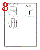
12 / 15 page  Application Information (Continued) easily satisfies the LM4914’s requirement for a dual switch headphone jack. For applications that require an SPDIF interface in the stereo headphone jack, use a Foxconn 2F1138-TJ-TR. SELECTING EXTERNAL COMPONENTS Input Capacitor Value Selection Amplifying the lowest audio frequencies requires high value input coupling capacitors (C 1 and C2 in Figure 2). A high value capacitor can be expensive and may compromise space efficiency in portable designs. In many cases, how- ever, the speakers used in portable systems, whether inter- nal or external, have little ability to reproduce signals below 150Hz. Applications using speakers with this limited fre- quency response reap little improvement by using large input capacitor. The LM4914’s advanced output transient suppression cir- cuitry has eliminated the need to select the input capacitor’s value in relation to the BYPASS capacitor’s value as was necessary in some previous Boomer amplifiers. The value of C 1 and C2 are now strictly determined by the desired low frequency response. As shown in Figure 2, the input resistors (R 1 and R2) and the input capacitors (C 1 and C2) produce a high pass filter cutoff frequency that is found using Equation (7). f C =1/2 πR iCi (7) As an example, when using a speaker with a low frequency limit of 150Hz, and input resistances (R 2 and R3) of 16.8k Ω, using Equation (7), input capacitances (C 1 and C2) are 0.063µF. The 0.1µF capacitors (C 1 and C2) shown in Figure 2 allow the LM4914 to drive high efficiency, full range speaker whose response extends below 30Hz. Bypass Capacitor Value Selection Besides minimizing the input capacitor size, careful consid- eration should be paid to value of C B, the capacitor con- nected to the BYPASS pin. Since C B determines how fast the LM4914 settles to quiescent operation, its value is critical when minimizing turn-on pops. The slower the LM4914’s outputs ramp to their quiescent DC voltage (nominally V DD/ 2), the smaller the turn-on pop. Choosing C B equal to 1.0µF along with a small value of Ci (in the range of 0.1µF to 0.39µF), produces a click-less and pop-less shutdown func- tion. As discussed above, choosing C i no larger than neces- sary for the desired bandwidth helps minimize clicks and pops. C B’s value should be in the range of 5 times to 7 times the value of C i. This ensures that output transients are eliminated when power is first applied or the LM4914 re- sumes operation after shutdown. OPTIMIZING CLICK AND POP REDUCTION PERFORMANCE The LM4914 contains circuitry that eliminates turn-on and shutdown transients ("clicks and pops") and transients that could occur when switching between BTL speakers and single-ended headphones. For this discussion, turn-on re- fers to either applying the power supply voltage or when the micro-power shutdown mode is deactivated. As the V DD/2 voltage present at the BYPASS pin ramps to its final value, the LM4914’s internal amplifiers are configured as unity gain buffers and are disconnected from the RO/MO+ and LO/MO- pins. An internal current source charges the capacitor connected between the BYPASS pin and GND in a controlled, linear manner. Ideally, the input and outputs track the voltage applied to the BYPASS pin. The gain of the internal amplifiers remains unity until the voltage on the bypass pin reaches V DD/2. As soon as the voltage on the bypass pin is stable, the device becomes fully operational and the amplifier outputs are reconnected to their respective output pins. Although the BYPASS pin current cannot be modified, changing the size of C B alters the device’s turn-on time. There is a linear relationship between the size of C B and the turn-on time. Here are some typical turn-on times for various values of C B: C B(µF) T ON (ms) 0.01 2 0.1 20 0.22 42 0.47 90 1.0 200 2.2 420 200634A2 FIGURE 4. Headphone Circuit www.national.com 12 |
|
|
Link URL |
| Czy Alldatasheet okazała się pomocna? [ DONATE ] |
O Alldatasheet | Reklama | Kontakt | Polityka prywatności | Link do karty katalogowej | Linki | Lista producentów All Rights Reserved©Alldatasheet.com |
| Russian : Alldatasheetru.com | Korean : Alldatasheet.co.kr | Spanish : Alldatasheet.es | French : Alldatasheet.fr | Italian : Alldatasheetit.com Portuguese : Alldatasheetpt.com | Polish : Alldatasheet.pl | Vietnamese : Alldatasheet.vn Indian : Alldatasheet.in | Mexican : Alldatasheet.com.mx | British : Alldatasheet.co.uk | New Zealand : Alldatasheet.co.nz |
|
Family Site : ic2ic.com |
icmetro.com |
 Polish ▼
 English
 Chinese
 German
 Japanese
 Russian
 Korean
 Spanish
 French
 Italian
 Portuguese
 Polish
 Vietnamese
 Indian
 Mexican
 British
 New Zealand