|
Zakładka z wyszukiwarką danych komponentów |
|
|
Zakładka z wyszukiwarką danych komponentów |
|
IRU3065 Arkusz danych(PDF) 6 Page - International Rectifier |
|
|
|||||||||||||||||||||||||||||
IRU3065 Arkusz danych(HTML) 6 Page - International Rectifier |
|
|
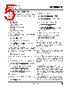
6 / 15 page  6 IRU3065(PbF) www.irf.com in figure 1. The schottky diode can be replaced with a 100Ω resistor (Figure 28.) with a small sacrifice of effi- ciency but lower cost. Thermal Consideration The thermal design is to ensure maximum junction tem- perature of IRU3065 will not exceed the maximum op- eration junction temperature, which is 125 C. The junc- tion temperature can be estimated by the following: TJ = PD×ΘJA+TA≤TJ(MAX) = 125 C Where ΘJA is the thermal resistance from junction to case which is usually provided in the specification. PD is the power dissipation. TA is the ambient temperature. The package thermal resistance of IRU3065 is estimated as 230C/W due to compact package. Assuming the maximum allowed ambient temperature is 70C, the maximum power dissipation of IRU3065 will be PD<(125-70C)/ΘJA=(125-70)/230=240mW For High Power Application The IR3065 driver is designed to driver PMOS for low current applications. Figure 4. shows the rise time ver- sus cap load. For big capacitor load, the rise time is increasing. Rise time versus cap load 0 10 20 30 40 50 60 70 80 90 00.511.522.5 Cap(nF) Fig.4. Rise time versus cap load. The internal gate driver of IRU3065 is designed for load current up to 1A. For higher power applications, external driver is recommended to driver the external FETs. Demo board Evaluation Results Fig.1 shows the evaluation board schematic and the selected components. The diode D1 can be replaced with a 100ohm resistor. The measured efficiency ver- sus load current is shown in Fig. 6. With the boot strap schottky diode, the efficiency is slight higher compar- ing with using 100ohm resistor. If higher efficiency is preferred, lower operation fre- quency should be selected. Figure. 5 shows a effi- ciency curve when 4.7uH inductor is chosen. The maxi- mum operation frequency reduces from 800k to 250kHz. As a results, efficiency is more than 10% higher. For the application circuit shown in Fig.1. The mea- sured output voltage versus output current is shown in Figure 7. When the load current approaches 400mA, the output voltage starts to drop and goes into power limit mode. When output is about 1A, the output voltage will goes almost zero. The measured frequency versus load is listed in Fig- ure 8. The highest switching frequency occurs at about 440mA. As load current goes up, the IC goes into power limit mode and frequency automatically goes down to protect the system. The current sensing comparator threshold voltage ver- sus VCC is shown in Figure. 9. Since this threshold is only a divided voltage of VCC, it will changes when VCC changes. This should be aware in the application. The output voltage versus Vin=VCC is shown in fig- ure 11. Since the voltage reference is set by Vin. When Vin changes, the output voltage will change along Vin. Sometimes this feature is preferrable since Vout may want to be tracked with Vin except the polarity. How- ever, if more accurate output is required, a external voltage reference should set the output voltage. For the evaluation board, the measured inductor volt- age waveforms are listed in Figure 13-17. Figure 15 shows the measured inductor voltage waveform when output current is 250mA, which the converter is oper- ated in regulation mode and output voltage is regulated at desired voltage -5V. Figure 16 shows the measured inductor voltage waveform when the output current is equal to the critical current IOCP. Figure 17 shows the measured inductor voltage waveform when the output is in short circuit, which indicates that the converter is in power limit mode and output voltage is near zero. . |
|
|
Link URL |
| Czy Alldatasheet okazała się pomocna? [ DONATE ] |
O Alldatasheet | Reklama | Kontakt | Polityka prywatności | Link do karty katalogowej | Linki | Lista producentów All Rights Reserved©Alldatasheet.com |
| Russian : Alldatasheetru.com | Korean : Alldatasheet.co.kr | Spanish : Alldatasheet.es | French : Alldatasheet.fr | Italian : Alldatasheetit.com Portuguese : Alldatasheetpt.com | Polish : Alldatasheet.pl | Vietnamese : Alldatasheet.vn Indian : Alldatasheet.in | Mexican : Alldatasheet.com.mx | British : Alldatasheet.co.uk | New Zealand : Alldatasheet.co.nz |
|
Family Site : ic2ic.com |
icmetro.com |
 Polish ▼
 English
 Chinese
 German
 Japanese
 Russian
 Korean
 Spanish
 French
 Italian
 Portuguese
 Polish
 Vietnamese
 Indian
 Mexican
 British
 New Zealand