|
Zakładka z wyszukiwarką danych komponentów |
|
|
Zakładka z wyszukiwarką danych komponentów |
|
OPAMP3EVB Arkusz danych(PDF) 6 Page - ON Semiconductor |
|
|
|||||||||||||||||||||||||||||
OPAMP3EVB Arkusz danych(HTML) 6 Page - ON Semiconductor |
|
|
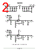
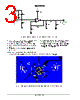
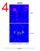
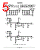
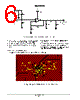
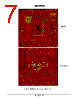
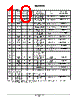
6 / 12 page  OPAMP3EVB http://onsemi.com 6 EN3 JMP3 BNC Connector Scope +IN3 J7 R19 R20 BNC Connector +IN3 J8 R27 + − R26 R24 C15 R21 R22 BNC Connector Out3 J9 VCC VEE 7 8 9 10 Figure 5. NCS2540 Evaluation Board Schematic (continued) • L1, L2, C1, C2, C3, C4, C5, C6, C7, C8, C11, C12, D6, D7, R5, and R7 are for power supply noise suppression. • R3, R18, R27 are for input matching of 50 W trace. • R1, R2, R8, R9, R19, R20 are for monitoring the input signal. • R4, R6 R15, R7, R24, R26 are for feedback resistor configuration. • C9, R10, R11, C10, R12, R13, C15, R21, R22 are for different loading configurations of the op amp. • Jumper 1 is for the enable pin of the device. They can be used to enable or disable the op amps. Board Layout (NCS2540DTBEVB) Figure 6 and 7 shows the board layout of the NCS2540DTBEVB device. Figure 6. Close Up of NCS2540DTBEVB Evaluation Board Layout |
|
|
Link URL |
| Czy Alldatasheet okazała się pomocna? [ DONATE ] |
O Alldatasheet | Reklama | Kontakt | Polityka prywatności | Link do karty katalogowej | Linki | Lista producentów All Rights Reserved©Alldatasheet.com |
| Russian : Alldatasheetru.com | Korean : Alldatasheet.co.kr | Spanish : Alldatasheet.es | French : Alldatasheet.fr | Italian : Alldatasheetit.com Portuguese : Alldatasheetpt.com | Polish : Alldatasheet.pl | Vietnamese : Alldatasheet.vn Indian : Alldatasheet.in | Mexican : Alldatasheet.com.mx | British : Alldatasheet.co.uk | New Zealand : Alldatasheet.co.nz |
|
Family Site : ic2ic.com |
icmetro.com |
 Polish ▼
 English
 Chinese
 German
 Japanese
 Russian
 Korean
 Spanish
 French
 Italian
 Portuguese
 Polish
 Vietnamese
 Indian
 Mexican
 British
 New Zealand