12 / 12 page

4-342
RF2878
Rev A0 060206
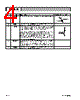
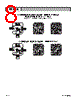
PCB Solder Mask Pattern
Liquid Photo-Imageable (LPI) solder mask is recommended. The solder mask footprint will match what is shown for the
PCB metal land pattern with a 2mil to 3mil expansion to accommodate solder mask registration clearance around all
pads. The center-grounding pad shall also have a solder mask clearance. Expansion of the pads to create solder mask
clearance can be provided in the master data or requested from the PCB fabrication supplier.
A
A
A
A
A
2.60
Pin 1
A = 0.90 x 1.20 (mm) Typ.
Pin 5
Dimensions in mm.
0.95 Typ.
1.90 Typ.
Figure 2. PCB Solder Mask (Top View)


 Polish ▼
 English
 Chinese
 German
 Japanese
 Russian
 Korean
 Spanish
 French
 Italian
 Portuguese
 Polish
 Vietnamese
 Indian
 Mexican
 British
 New Zealand