4-334
RF2878
Rev A0 060206
Pin
Function
Description
Interface Schematic
1RF IN
RF input pin. This pin is DC coupled and matched to 50
Ω at 836 MHz.
2
GND1
Ground connection. For best performance, keep traces physically short
and connect immediately to ground plane.
3
VPD
For low noise amplifier applications, this pin is used to control the bias
current. See plots for bias current settings. An external resistor (R1)
can be used to set the bias current for any VPD voltage.
For driver amplifier applications, this is the Power Down pin for the IC.
VPD=2.8V +/- 0.1V is required for proper operation. VPD< 0.9V turns
off the Part. External RF bypassing is required. The trace length
between the pin and the bypass capacitors should be minimized. The
ground side of the bypass capacitors should connect immediately to
ground plane. Nominal current required for VPD=2.8V is 2.0mA typical
and 3.0mA Max (@ VPD=2.9V).
4RF OUT
Amplifier Output pin. This pin is an open-collector output. It must be
biased to either VCC or pin 4 through a choke or matching inductor.
This pin is typically matched to 50
Ω with a shunt bias/matching induc-
tor and series blocking/matching capacitor. Refer to application sche-
matics.
5
GND2
Ground connection. For best performance, keep traces physically short
and connect immediately to ground plane.
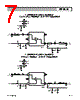
RF IN
RF OUT
To Bias
Circuit
PD


 Polish ▼
 English
 Chinese
 German
 Japanese
 Russian
 Korean
 Spanish
 French
 Italian
 Portuguese
 Polish
 Vietnamese
 Indian
 Mexican
 British
 New Zealand