|
Zakładka z wyszukiwarką danych komponentów |
|
|
Zakładka z wyszukiwarką danych komponentów |
|
CLC730131 Arkusz danych(PDF) 5 Page - National Semiconductor (TI) |
|
|
|
|||||||||||||||||||||||||||||
CLC730131 Arkusz danych(HTML) 5 Page - National Semiconductor (TI) |
|
|
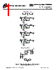
5 / 8 page  © 2002 National Semiconductor Corporation www.national.com 5 CLC730131 evaluation board is configured for non-inverting gain. However, it is possible to configure the board for inverting gain. To convert to inverting gain, do the following changes: How to convert the board for Inverting Gain: 1. Cut RT1 from ground plane by cutting trace going from RT1 (terminal closest to RG1) to the top ground plane. See drawing above. 2. Cut RIN1 from input signal trace by cutting trace going from RIN1 (terminal closest to RG1) to the input signal trace, see drawing above. 3. Add jumper wire from input signal trace to trace connecting RG1 to RT1, see drawing above. Changes shown for channel 1 only. Repeat these steps on the corresponding components for the other three channels. Fig. 5: Details of Modification to Inverting Gain |
|
|
Link URL |
| Czy Alldatasheet okazała się pomocna? [ DONATE ] |
O Alldatasheet | Reklama | Kontakt | Polityka prywatności | Link do karty katalogowej | Linki | Lista producentów All Rights Reserved©Alldatasheet.com |
| Russian : Alldatasheetru.com | Korean : Alldatasheet.co.kr | Spanish : Alldatasheet.es | French : Alldatasheet.fr | Italian : Alldatasheetit.com Portuguese : Alldatasheetpt.com | Polish : Alldatasheet.pl | Vietnamese : Alldatasheet.vn Indian : Alldatasheet.in | Mexican : Alldatasheet.com.mx | British : Alldatasheet.co.uk | New Zealand : Alldatasheet.co.nz |
|
Family Site : ic2ic.com |
icmetro.com |
 Polish ▼
 English
 Chinese
 German
 Japanese
 Russian
 Korean
 Spanish
 French
 Italian
 Portuguese
 Polish
 Vietnamese
 Indian
 Mexican
 British
 New Zealand