|
Zakładka z wyszukiwarką danych komponentów |
|
|
Zakładka z wyszukiwarką danych komponentów |
|
LTC1422 Arkusz danych(PDF) 8 Page - Linear Technology |
|
|
|||||||||||||||||||||||||||||
LTC1422 Arkusz danych(HTML) 8 Page - Linear Technology |
|
|
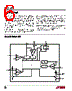
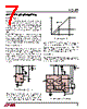
8 / 16 page  8 LTC1422 APPLICATIONS INFORMATION VOUT TIMER RESET V2 V2 V2 V1 V1 1.232V 1.232V 12 3 4 1422 F04 Figure 4. Supply Monitor Waveforms When the voltage at the FB pin rises above its reset threshold (1.232V), the comparator COMP 2 output goes high, and a timing cycle starts (Figure 4, time points 1 and 4). After a complete timing cycle, RESET is pulled high. The 12 µA pull-up current source to VCC on RESET has a series diode so the pin can be pulled above VCC by an external pull-up resistor without forcing current back into supply. When the supply voltage at the FB pin drops below its reset threshold, the comparator Comp 2 output goes low. After passing through a glitch filter, RESET is pulled low (time point 2). If the FB pin rises above the reset threshold for less than a timing cycle, the RESET output will remain low (time point 3). Glitch Filter The LTC1422 has a glitch filter to prevent RESET from generating a system reset when there are transients on the FB pin. The filter is 20 µs for large transients (greater than 150mV) and up to 80 µs for small transients. The relation- ship between glitch filter time and the transient voltage is shown in Typical Performance curve: Glitch Filter Time vs Feedback Transient. Soft Reset In some cases a system reset is desired without a power down. The ON pin can signal the RESET pin to go low without turning off the external N-channel (a soft reset). This is accomplished by holding the ON pin low for only 15 µs or less (Figure 5, time point 1). At about 30µs from the falling edge of the ON pin (time point 2) the RESET pin goes low and stays low for one timing cycle. Figure 5. Soft Reset Waveforms RESET VOUT GATE 1422 F05 TIMER ON 30 µs 12 30 µs 34 6 5 15 µs 20 µs If the ON pin is held low for longer than 40 µs, the gate will turn off and the RESET pin will eventually go low (time points 4, 5 and 6). Timer The system timing for the LTC1422 is generated by the circuitry shown in Figure 6. The timer is used to set the turn-on delay after the ON pin goes high and the delay before the RESET pin goes high after the output supply voltage is good as sensed by the FB pin. + SENSE TIMER 2 µA R4 R3 R2 7 VCC VOUT VCC 8 GATE LTC1422 6 2 ON 1422 F06 SUPPLY MONITOR 1 5 C2 3 4 RESET C1 CLOAD Q2 R1 LOGIC 1.232V – + COMP 4 Q1 Figure 6. System Timing Block Diagram |
|
|
Link URL |
| Czy Alldatasheet okazała się pomocna? [ DONATE ] |
O Alldatasheet | Reklama | Kontakt | Polityka prywatności | Link do karty katalogowej | Linki | Lista producentów All Rights Reserved©Alldatasheet.com |
| Russian : Alldatasheetru.com | Korean : Alldatasheet.co.kr | Spanish : Alldatasheet.es | French : Alldatasheet.fr | Italian : Alldatasheetit.com Portuguese : Alldatasheetpt.com | Polish : Alldatasheet.pl | Vietnamese : Alldatasheet.vn Indian : Alldatasheet.in | Mexican : Alldatasheet.com.mx | British : Alldatasheet.co.uk | New Zealand : Alldatasheet.co.nz |
|
Family Site : ic2ic.com |
icmetro.com |
 Polish ▼
 English
 Chinese
 German
 Japanese
 Russian
 Korean
 Spanish
 French
 Italian
 Portuguese
 Polish
 Vietnamese
 Indian
 Mexican
 British
 New Zealand