|
Zakładka z wyszukiwarką danych komponentów |
|
|
Zakładka z wyszukiwarką danych komponentów |
|
AN-733 Arkusz danych(PDF) 2 Page - Analog Devices |
|
|
|||||||||||||||||||||||||||||
AN-733 Arkusz danych(HTML) 2 Page - Analog Devices |
|
|
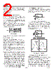
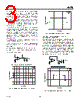
2 / 4 page  –2– AN-733 The algebraic sum of these two components should be equal to VOUT. By applying the principles expressed in the output voltage VOUT components, and by letting R4 = R2 and R7 = R6, then: VOUT1 = VIN1 R7/R2 VOUT2 = –VIN2 R7/R2 VOUT = VOUT1 + VOUT2 = ( VIN1 – VIN2) R7/R1 Difference amplifiers are commonly used in high accuracy circuits to improve the common-mode rejec- tion ratio, typically known as CMRR. For this type of application, CMRR depends upon how tightly matched resistors are used; poorly matched resis- tors result in a low value of CMRR. To see how this works, consider a hypothetical source of error for resistor R7 (1 – error). Using the superposi- tion principle and letting R4 = R2 and R7 = R6, the output voltage would be as follows: V R R R R R R error VD R R R error OUT = − + + × + + × 7 2 1 2 2 7 2 7 2 7 2 7 V V V DD IN IN = − 2 1 From this equation, ACM and ADM can be defined as follows: ACM = R7/(R7 – R2) error ADM = R7/R2 {1 – [(R2+2R7/R2+R7) error/2]} These equations demonstrate that when there is not an error in the resistor values, the ACM = 0 and the amplifier responds only to the differential voltage being applied to its inputs; under these conditions, the CMRR of the circuit becomes highly dependent on the CMRR of the amplifier selected for this job. As mentioned above, errors introduced by resistor mismatch can be a big drawback of discrete differential amplifiers, but there are different ways to optimize this circuit configuration: 1. The differential gain is directly related to the ratio R7/R2; therefore, one way to optimize the perfor- mance of this circuit is to place the amplifier in a high gain configuration. When larger values for resistors R7 and R6 and smaller values for resistors R2 and R4 are selected, the higher the gain, the higher the CMRR. For example, when R7 = R6 = 10 k, and R2 = R4 = 1 k, and error = 0.1%, CMRR improves to better than 80 dB. For high gain configuration, select amplifiers with very low IBIAS and very high gain (such as the AD8551, AD8571, AD8603, and AD8605) to reduce errors. 2. Select resistors that have much tighter tolerance and accuracy. The more closely they are matched, the better the CMRR. For example, if a CMRR of 90 dB is needed, then match resistors to approximately 0.02%. CURRENT-TO-VOLTAGE CONVERTER Current may be measured in two ways with an opera- tional amplifier: It can be converted to a voltage with a resistor and then amplified, or injected directly into a summing node. ���� �� �� ���� ���� � ���� � �� Figure 3. Current-to-Voltage Converter Figure 3 is a typical representation of a current-to-voltage transducer. The input current is fed directly into the sum- ming node and the amplifier output voltage changes to exactly the same current from the summing node through R7. The scale factor of this circuit is R7 volts per amps. The only conversion error in this circuit is IBIAS, which is summed algebraically with IIN. ���� �� �� �� �� �� �� �� �� ��� � ��� ��� � ��� Figure 5. Output Response GENERATION OF SQUARE WAVEFORMS USING A BISTABLE MULTIVIBRATOR A square waveform can be simply generated by arrang- ing the amplifier for a bistable multivibrator to switch states periodically as Figure 5 shows. Once the output of the amplifier reaches one of two pos- sible levels, such as L+, capacitor C9 charges toward this level through resistor R7. The voltage across C9, which is applied to the negative input terminal of the ampli- fier denoted as V–, then rises exponentially toward L+ with a time constant = C9R7. Meanwhile, the voltage REV. A |
|
|
Link URL |
| Czy Alldatasheet okazała się pomocna? [ DONATE ] |
O Alldatasheet | Reklama | Kontakt | Polityka prywatności | Link do karty katalogowej | Linki | Lista producentów All Rights Reserved©Alldatasheet.com |
| Russian : Alldatasheetru.com | Korean : Alldatasheet.co.kr | Spanish : Alldatasheet.es | French : Alldatasheet.fr | Italian : Alldatasheetit.com Portuguese : Alldatasheetpt.com | Polish : Alldatasheet.pl | Vietnamese : Alldatasheet.vn Indian : Alldatasheet.in | Mexican : Alldatasheet.com.mx | British : Alldatasheet.co.uk | New Zealand : Alldatasheet.co.nz |
|
Family Site : ic2ic.com |
icmetro.com |
 Polish ▼
 English
 Chinese
 German
 Japanese
 Russian
 Korean
 Spanish
 French
 Italian
 Portuguese
 Polish
 Vietnamese
 Indian
 Mexican
 British
 New Zealand