|
Zakładka z wyszukiwarką danych komponentów |
|
|
Zakładka z wyszukiwarką danych komponentów |
|
AN-733 Arkusz danych(PDF) 3 Page - Analog Devices |
|
|
|||||||||||||||||||||||||||||
AN-733 Arkusz danych(HTML) 3 Page - Analog Devices |
|
|
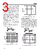
3 / 4 page  –3– AN-733 at the positive input terminal of the amplifier, denoted as V+ = BL+. This continues until the capacitor voltage reaches the positive threshold VTH, at which point the bistable multivibrator switches to the other stable state in which VO = L– and V+ = BL–. This is shown in Figure 5. The capacitor then begins to discharge, and its voltage, V–, decreases exponentially toward L–. This continues until V– reaches the negative threshold VTL, at which time the bistable multivibrator switches to the positive output state, and the cycle repeats itself. It is important to note that the frequency of the square wave being generated, fO, depends only on the external components being used. Any variation in L+ will cause V+ to vary in proportion, ensuring the same transition time and the same oscillation frequency. The maximum operating frequency is determined by the amplifier speed, which can be increased significantly by using faster devices. The lowest operating frequency depends on the practical upper limits set by R7 and C9. Using the name convention outlined on the PRA OPAMP evaluation board, the circuit should be connected as follows: B = R4/(R4 + R9); feedback factor (noninverting input) T = 2R7 C9 ln((1 + B)/(1 – B)); period of oscillation fO = 1/T; oscillation frequency ���� ��� ��� �� �� Figure 6. Series Resistor Compensation ��� ���� ���������� �� � ���� �� � ��� Figure 7. Capacitive Load Drive Without Resistor ��� ���� ���������� �� � ���� �� � ��� Figure 8. Capacitive Load Drive with Resistor EXTERNAL COMPENSATION TECHNIQUES Series Resistor Compensation The use of external compensation networks may be required to optimize certain applications. Figure 6 is a typical representation of a series resistor compensation for stabilizing an op amp driving capacitive load. The sta- bilizing effect of the series resistor isolates the op amp output and the feedback network from the capacitive load. The required amount of series resistance depends on the part used, but values of 5 to 50 are usually sufficient to prevent local resonance. The disadvantages of this technique are a reduction in gain accuracy and extra distortion when driving nonlinear loads. ���� ��� �� �� �� �� ��� ���� ���������� Figure 10. Capacitive Load Drive Without Snubber REV. A |
|
|
Link URL |
| Czy Alldatasheet okazała się pomocna? [ DONATE ] |
O Alldatasheet | Reklama | Kontakt | Polityka prywatności | Link do karty katalogowej | Linki | Lista producentów All Rights Reserved©Alldatasheet.com |
| Russian : Alldatasheetru.com | Korean : Alldatasheet.co.kr | Spanish : Alldatasheet.es | French : Alldatasheet.fr | Italian : Alldatasheetit.com Portuguese : Alldatasheetpt.com | Polish : Alldatasheet.pl | Vietnamese : Alldatasheet.vn Indian : Alldatasheet.in | Mexican : Alldatasheet.com.mx | British : Alldatasheet.co.uk | New Zealand : Alldatasheet.co.nz |
|
Family Site : ic2ic.com |
icmetro.com |
 Polish ▼
 English
 Chinese
 German
 Japanese
 Russian
 Korean
 Spanish
 French
 Italian
 Portuguese
 Polish
 Vietnamese
 Indian
 Mexican
 British
 New Zealand