|
Zakładka z wyszukiwarką danych komponentów |
|
|
Zakładka z wyszukiwarką danych komponentów |
|
LTM4602 Arkusz danych(PDF) 13 Page - Linear Technology |
|
|
|||||||||||||||||||||||||||||
LTM4602 Arkusz danych(HTML) 13 Page - Linear Technology |
|
|
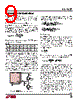
13 / 24 page  LTM4602 13 4602fa Enable The RUN/SS pin can be driven from logic as shown in Figure 5. This function allows the LTM4602 to be turned on or off remotely. The ON signal can also control the sequence of the output voltage. Figure 5. Enable Circuit with External Logic Figure 6. Output Voltage Tracking with the LTC2923 Controller Output Voltage Tracking For the applications that require output voltage tracking, several LTM4602 modules can be programmed by the power supply tracking controller such as the LTC2923. Figure 6 shows a typical schematic with LTC2923. Coin- cident, ratiometric and offset tracking for VOUT rising and falling can be implemented with different sets of resistor values. See the LTC2923 data sheet for more details. EXTVCC Connection An internal low dropout regulator produces an internal 5V supply that powers the control circuitry and FET drivers. Therefore, if the system does not have a 5V power rail, the LTM4602 can be directly powered by VIN. The gate driver current through LDO is about 18mA. The internal LDO power dissipation can be calculated as: PLDO_LOSS = 18mA • (VIN – 5V) The LTM4602 also provides an external gate driver volt- age pin EXTVCC. If there is a 5V rail in the system, it is recommended to connect EXTVCC pin to the external 5V rail. Whenever the EXTVCC pin is above 4.7V, the inter- nal 5V LDO is shut off and an internal 50mA P-channel switch connects the EXTVCC to internal 5V. Internal 5V is supplied from EXTVCC until this pin drops below 4.5V. Do not apply more than 6V to the EXTVCC pin and ensure that EXTVCC < VIN. The following list summaries the possible connections for EXTVCC: 1. EXTVCC grounded. Internal 5V LDO is always powered from the internal 5V regulator. 2. EXTVCC connected to an external supply. Internal LDO is shut off. A high efficiency supply compatible with the MOSFET gate drive requirements (typically 5V) can im- prove overall efficiency. With this connection, it is always required that the EXTVCC voltage can not be higher than VIN pin voltage. Discontinuous Operation and FCB Pin The FCB pin determines whether the internal bottom MOSFET remains on when the inductor current reverses. There is an internal 4.75k pull-down resistor connecting this pin to ground. The default light load operation mode is forced continuous (PWM) current mode. This mode provides minimum output voltage ripple. In the application where the light load efficiency is im- portant, tying the FCB pin above 0.6V threshold enables discontinuous operation where the bottom MOSFET turns off when inductor current reverses. Therefore, the conduc- RUN/SS 4602 F05 LTM4602 PGND 2N7002 SGND ON Q1 VCC VIN VIN RONB VIN 5V RTB1 RTB2 RSET 49.9k 1.8V 3.3V RTA2 RTA1 RONA ON RAMPBUF TRACK1 TRACK2 FB1 GATE LTC2923 GND 4602 F06 RAMP RSET 66.5k 1.5V LTM4602 VIN VOUT LTM4602 DC/DC VIN VOUT VOSET VOSET FB2 SDO STATUS APPLICATIONS INFORMATION |
|
|
Link URL |
| Czy Alldatasheet okazała się pomocna? [ DONATE ] |
O Alldatasheet | Reklama | Kontakt | Polityka prywatności | Link do karty katalogowej | Linki | Lista producentów All Rights Reserved©Alldatasheet.com |
| Russian : Alldatasheetru.com | Korean : Alldatasheet.co.kr | Spanish : Alldatasheet.es | French : Alldatasheet.fr | Italian : Alldatasheetit.com Portuguese : Alldatasheetpt.com | Polish : Alldatasheet.pl | Vietnamese : Alldatasheet.vn Indian : Alldatasheet.in | Mexican : Alldatasheet.com.mx | British : Alldatasheet.co.uk | New Zealand : Alldatasheet.co.nz |
|
Family Site : ic2ic.com |
icmetro.com |
 Polish ▼
 English
 Chinese
 German
 Japanese
 Russian
 Korean
 Spanish
 French
 Italian
 Portuguese
 Polish
 Vietnamese
 Indian
 Mexican
 British
 New Zealand