|
Zakładka z wyszukiwarką danych komponentów |
|
|
Zakładka z wyszukiwarką danych komponentów |
|
NCP2809 Arkusz danych(PDF) 4 Page - ON Semiconductor |
|
|
|||||||||||||||||||||||||||||
NCP2809 Arkusz danych(HTML) 4 Page - ON Semiconductor |
|
|
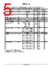
4 / 22 page  NCP2809 Series http://onsemi.com 4 PIN FUNCTION DESCRIPTION Pin Type Symbol Description 1 I IN_R Negative input of the second amplifier. It receives the audio input signal. Connected to the input capicator Cin (NCP2809A) or the external Rin (NCP2809B). 2 I SHUTDOWN The device enters in shutdown mode when a a low level is applied on this pin. 3 I BYPASS Bypass capacitor pin which provides the common mode voltage (VP/2). 4 O REF_I Virtual ground amplifier feed back. This pin sets the stereo headset ground. In order to improve crosstalk, this pin must be connected as close as possible to the ground connection of the headset (ideally at the ground pin of the headset connector). When one uses bypassing capacitors, this pin must be left unconnected. 5 I IN_L Negative input of the first amplifier. It receives the audio input signal. Connected to the input capacitor Cin (NCP2809A) or the external Rin (NCP2809B). 6 O OUT_L Stereo headset amplifier analog output left. This pin will output the amplified analog signal and, depending on the application, must be coupled with a capacitor or directly connected to the left loudspeaker of the headset. This output is able to drive a 16 W load in a single−ended configuration. 7 I VP Positive analog supply of the cell. Range: 2.2 V – 5.5 V 8 O OUT_I Virtual ground for stereo Headset common connection. This pin is directly connected to the common connection of the headset when use of bypassing capacitor is not required. When one uses bypassing capacitors, this pin must be left unconnected. 9 I VM Analog Ground 10 O OUT_R Stereo headset amplifier analog output right. This pin will output the amplified analog signal and, depending on the application, must be coupled with a capacitor or directly connected to the right loudspeaker of the headset. This output is able to drive a 16 W load in a single−ended configuration. MAXIMUM RATINGS (TA = +25°C) Rating Symbol Value Unit Supply Voltage Vp 6.0 V Operating Supply Voltage Op Vp 2.2 to 5.5 V Input Voltage Vin −0.3 to VCC + 0.3 V Max Output Current Iout 250 mA Power Dissipation Pd Internally Limited − Operating Ambient Temperature TA −40 to +85 °C Max Junction Temperature TJ 150 °C Storage Temperature Range Tstg −65 to +150 °C Thermal Resistance, Junction−to−Air RqJA 200 °C/W ESD Protection Human Body Model (HBM) (Note 1) Machine Model (MM) (Note 2) − 8000 200 V Latch up current at Ta = 85 _C (Note 3) ±100 mA Maximum ratings applied to the device are individual stress limit values (not normal operating conditions) and are not valid simultaneously. If stress limits are exceeded device functional operation is not implied, damage may occur and reliability may be affected. Functional operation should be restricted to the Recommended Operating Conditions. 1. Human Body Model, 100 pF discharged through a 1.5 k W resistor following specification JESD22/A114 8.0 kV can be applied on OUT_L, OUT_R, REF_I and OUT_I outputs. For other pins, 2.0 kV is the specified voltage. 2. Machine Model, 200 pF discharged through all pins following specification JESD22/A115. 3. Maximum ratings per JEDEC standard JESD78. *This device contains 752 active transistors and 1740 MOS gates. |
|
|
Link URL |
| Czy Alldatasheet okazała się pomocna? [ DONATE ] |
O Alldatasheet | Reklama | Kontakt | Polityka prywatności | Link do karty katalogowej | Linki | Lista producentów All Rights Reserved©Alldatasheet.com |
| Russian : Alldatasheetru.com | Korean : Alldatasheet.co.kr | Spanish : Alldatasheet.es | French : Alldatasheet.fr | Italian : Alldatasheetit.com Portuguese : Alldatasheetpt.com | Polish : Alldatasheet.pl | Vietnamese : Alldatasheet.vn Indian : Alldatasheet.in | Mexican : Alldatasheet.com.mx | British : Alldatasheet.co.uk | New Zealand : Alldatasheet.co.nz |
|
Family Site : ic2ic.com |
icmetro.com |
 Polish ▼
 English
 Chinese
 German
 Japanese
 Russian
 Korean
 Spanish
 French
 Italian
 Portuguese
 Polish
 Vietnamese
 Indian
 Mexican
 British
 New Zealand