|
Zakładka z wyszukiwarką danych komponentów |
|
|
Zakładka z wyszukiwarką danych komponentów |
|
PIC12F615 Arkusz danych(PDF) 15 Page - Microchip Technology |
|
|
|||||||||||||||||||||||||||||
PIC12F615 Arkusz danych(HTML) 15 Page - Microchip Technology |
|
|
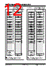
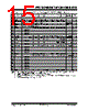
15 / 168 page  © 2006 Microchip Technology Inc. Preliminary DS41302A-page 13 PIC12F609/615/12HV609/615 TABLE 2-3: PIC12F609/HV609 SPECIAL FUNCTION REGISTERS SUMMARY BANK 1 Addr Name Bit 7 Bit 6 Bit 5 Bit 4 Bit 3 Bit 2 Bit 1 Bit 0 Value on POR, BOR Page Bank 1 80h INDF Addressing this location uses contents of FSR to address data memory (not a physical register) xxxx xxxx 22, 101 81h OPTION_REG GPPU INTEDG T0CS T0SE PSA PS2 PS1 PS0 1111 1111 16, 101 82h PCL Program Counter’s (PC) Least Significant Byte 0000 0000 22, 101 83h STATUS IRP(1) RP1(1) RP0 TO PD ZDC C 0001 1xxx 15, 101 84h FSR Indirect Data Memory Address Pointer xxxx xxxx 22, 101 85h TRISIO — — TRISIO5 TRISIO4 TRISIO3(4) TRISIO2 TRISIO1 TRISIO0 --11 1111 31, 101 86h — Unimplemented — — 87h — Unimplemented — — 88h — Unimplemented — — 89h — Unimplemented — — 8Ah PCLATH — — — Write Buffer for upper 5 bits of Program Counter ---0 0000 22, 101 8Bh INTCON GIE PEIE T0IE INTE GPIE T0IF INTF GPIF(3) 0000 0000 17, 101 8Ch PIE1 — — — —CMIE — —TMR1IE ---- 0--0 18, 101 8Dh — Unimplemented — — 8Eh PCON — — — — — —POR BOR ---- --qq 20, 101 8Fh — Unimplemented — — 90h OSCTUNE — — — TUN4 TUN3 TUN2 TUN1 TUN0 ---0 0000 29, 101 91h — Unimplemented — — 92h — Unimplemented — — 93h — Unimplemented — — 94h — Unimplemented — — 95h WPU(2) — —WPU5 WPU4 — WPU2 WPU1 WPU0 --11 -111 34, 101 96h IOC — — IOC5 IOC4 IOC3 IOC2 IOC1 IOC0 --00 0000 34, 101 97h — Unimplemented — — 98h — Unimplemented — — 99h — Unimplemented — — 9Ah — Unimplemented — — 9Bh — Unimplemented — — 9Ch — Unimplemented — — 9Dh — Unimplemented — — 9Eh — Unimplemented — — 9Fh ANSEL — — — —ANS3 — ANS1 ANS0 ---- 1-11 33, 101 Legend: – = Unimplemented locations read as ‘0’, u = unchanged, x = unknown, q = value depends on condition, shaded = unimplemented Note 1: IRP and RP1 bits are reserved, always maintain these bits clear. 2: GP3 pull-up is enabled when MCLRE is ‘1’ in the Configuration Word register. 3: MCLR and WDT Reset does not affect the previous value data latch. The GPIF bit will clear upon Reset but will set again if the mismatch exists. 4: TRISIO3 always reads as ‘1’ since it is an input only pin. |
|
Link URL |
| Czy Alldatasheet okazała się pomocna? [ DONATE ] |
O Alldatasheet | Reklama | Kontakt | Polityka prywatności | Link do karty katalogowej | Linki | Lista producentów All Rights Reserved©Alldatasheet.com |
| Russian : Alldatasheetru.com | Korean : Alldatasheet.co.kr | Spanish : Alldatasheet.es | French : Alldatasheet.fr | Italian : Alldatasheetit.com Portuguese : Alldatasheetpt.com | Polish : Alldatasheet.pl | Vietnamese : Alldatasheet.vn Indian : Alldatasheet.in | Mexican : Alldatasheet.com.mx | British : Alldatasheet.co.uk | New Zealand : Alldatasheet.co.nz |
|
Family Site : ic2ic.com |
icmetro.com |
 Polish ▼
 English
 Chinese
 German
 Japanese
 Russian
 Korean
 Spanish
 French
 Italian
 Portuguese
 Polish
 Vietnamese
 Indian
 Mexican
 British
 New Zealand