|
Zakładka z wyszukiwarką danych komponentów |
|
|
Zakładka z wyszukiwarką danych komponentów |
|
45111 Arkusz danych(PDF) 150 Page - List of Unclassifed Manufacturers |
|
|
|||||||||||||||||||||||||||||
45111 Arkusz danych(HTML) 150 Page - List of Unclassifed Manufacturers |
|
|
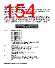
150 / 184 page  15 Appendix E: SX Data Sheet Page 150 • SX-Key/Blitz Development System Manual 2.0 • Parallax, Inc. Table 29 - SX Pins Name Type Input Levels Description RA0 – RA7* I/O TTL/CMOS Bi-directional I/O Pin, Complimentary Drive RB0 - RB2 I/O TTL/CMOS/ST Bi-directional I/O Pin; MIWU mode; Comparator output, - input, + input RB3 - RB7 I/O TTL/CMOS/ST Bi-directional I/O Pin; MIWU mode; (SX48/52 RB4 – RB7: T1 capture input 1, 2, PWM/compare out, ext. clock source) RC0 - RC7* I/O TTL/CMOS/ST Bi-directional I/O Pin (SX48/52 RC0 – RC3: T2 capture input 1, 2, PWM/compare out, external clock source) RD0 – RE7* I/O TTL/CMOS/ST Bi-directional I/O Pin RTCC I ST Input to Real Time Clock/Counter MCLR I ST Master Clear (reset) input (active low). OSC1 I ST Oscillator crystal input - external clock input. OSC2 I/O CMOS Weakly pulled to Vdd internally on RC mode. Vdd P - Positive supply for logic and I/O pins. Vss P - Ground Reference for logic and I/O pins. * RA4 – RA7 is only available on the SX52, RD0 – RE7 are only available on the SX48/52, RC0 – RC7 is not available on the SX18/20 15.2 Architecture The Ubicom SX chip offers 2K x 12 internal EE/Flash program memory (4K x 12 in the SX48/52) and up to 137 bytes of general purpose RAM memory (262 bytes in the SX48/52). The EE/Flash memory is organized in 512-word pages. The RAM memory is addressable directly or indirectly (as well as semi- directly in the SX48/52). All special function registers are mapped into the data memory. Configuration registers do not appear in data memory and are only accessible through the use of the MODE register and the port configuration commands. The ALU is 8-bits wide and is capable of arithmetic and Boolean operations. The ‘W’ register is the working register for the ALU. Typically, it holds one operand in a two-operand instruction. Depending on the instruction executed, the ALU may affect the values of the Carry (C), Zero (Z), and Digit Carry (DC) flags of the STATUS register. The SX chip comes equipped with special features that reduce system cost and power requirements. The Power-On Reset (POR) and Device Reset Timer eliminate the need for external reset circuitry. The power saving SLEEP mode, watchdog timer, and code protect features reduce system cost and improve system integrity. |
|
Link URL |
| Czy Alldatasheet okazała się pomocna? [ DONATE ] |
O Alldatasheet | Reklama | Kontakt | Polityka prywatności | Link do karty katalogowej | Linki | Lista producentów All Rights Reserved©Alldatasheet.com |
| Russian : Alldatasheetru.com | Korean : Alldatasheet.co.kr | Spanish : Alldatasheet.es | French : Alldatasheet.fr | Italian : Alldatasheetit.com Portuguese : Alldatasheetpt.com | Polish : Alldatasheet.pl | Vietnamese : Alldatasheet.vn Indian : Alldatasheet.in | Mexican : Alldatasheet.com.mx | British : Alldatasheet.co.uk | New Zealand : Alldatasheet.co.nz |
|
Family Site : ic2ic.com |
icmetro.com |
 Polish ▼
 English
 Chinese
 German
 Japanese
 Russian
 Korean
 Spanish
 French
 Italian
 Portuguese
 Polish
 Vietnamese
 Indian
 Mexican
 British
 New Zealand