|
Zakładka z wyszukiwarką danych komponentów |
|
|
Zakładka z wyszukiwarką danych komponentów |
|
45111 Arkusz danych(PDF) 151 Page - List of Unclassifed Manufacturers |
|
|
|||||||||||||||||||||||||||||
45111 Arkusz danych(HTML) 151 Page - List of Unclassifed Manufacturers |
|
|
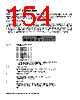
151 / 184 page  15 Appendix E: SX Data Sheet SX-Key/Blitz Development System Manual 2.0 • Parallax, Inc. • Page 151 15.2.1 Instruction Pipeline Figure 20 - Instruction Pipeline There are several stages an instruction must go through to actually execute within the SX chip. Specifically, there are four stages that are collectively referred to as the pipeline, and are shown in Figure 20 - Instruction Pipeline . The first instruction is fetched from memory on the first clock cycle. On the second clock cycle the first instruction is decoded and the second instruction is fetched. On the third clock cycle the first instruction is executed, the second instruction is decoded, and the third instruction is fetched. On the fourth clock cycle the first instruction’s results are written to its destination, the second instruction is executed, the third instruction is decoded and the fourth instruction is fetched. Once the pipeline is full, instructions are executed at the rate of one per clock cycle (in Turbo mode). Instructions that directly alter the value in the program counter, i.e. jumps, calls, etc. require that the pipeline be cleared and subsequently refilled. When the pipeline is cleared, the fetch and decode stages are replaced with ‘nop’ instructions. This effectively nullifies the invalid instructions and increases the cycle-time for that command by 3 cycles. 15.2.2 Read-Modify-Write Considerations Use caution when performing successive SETB or CLRB operations on an I/O port pin. Since input data used for an instruction must be valid during the time the instruction is executed, and the result output from an instruction is valid after that instruction completes its operation, unexpected results from successive read-modify-write operations on I/O pins can occur when the SX is running at extremely high speeds. The SX has an internal write-back section to prevent such data errors from occurring but it is recommended that you buffer successive read-modify-write instructions performed on I/O pins of the same port at extremely high clock rates with a ‘nop’ instruction. Also note, a read of an I/O pin actually reads the pin, not the output data latch. That is, if an output driver on a pin is enabled and driven high, but the external circuit is holding it low, a read of the port pin will indicate that the pin is low. Of course, externally driving an I/O pin while the output latch is driving it will result in damage to the SX chip. Care should be taken to not do this. 15.2.3 Register Map Structure The SX20/28 RAM memory consists of a global bank of special function registers and eight banks of 16 general-purpose registers. The SX48/52 RAM memory consists of a global bank of special function registers and 16 banks of 16 general-purpose registers. Figure 21 – SX20/28 Register Map and Figure 22 Fetch Decode Execute Write Stage of Instruction State of Clock Clock Cycle 1 Clock Cycle 2 Clock Cycle 3 Clock Cycle 4 |
|
Link URL |
| Czy Alldatasheet okazała się pomocna? [ DONATE ] |
O Alldatasheet | Reklama | Kontakt | Polityka prywatności | Link do karty katalogowej | Linki | Lista producentów All Rights Reserved©Alldatasheet.com |
| Russian : Alldatasheetru.com | Korean : Alldatasheet.co.kr | Spanish : Alldatasheet.es | French : Alldatasheet.fr | Italian : Alldatasheetit.com Portuguese : Alldatasheetpt.com | Polish : Alldatasheet.pl | Vietnamese : Alldatasheet.vn Indian : Alldatasheet.in | Mexican : Alldatasheet.com.mx | British : Alldatasheet.co.uk | New Zealand : Alldatasheet.co.nz |
|
Family Site : ic2ic.com |
icmetro.com |
 Polish ▼
 English
 Chinese
 German
 Japanese
 Russian
 Korean
 Spanish
 French
 Italian
 Portuguese
 Polish
 Vietnamese
 Indian
 Mexican
 British
 New Zealand