 |
Zakładka z wyszukiwarką danych komponentów |
|
|
Zakładka z wyszukiwarką danych komponentów |
|
The question interval is too short.
Please try again in a few seconds.

Hello, Please ask a question about ADRF6614-EVALZ Datasheet
# Example questions:
➢ What is the typical integrated phase noise (from 1 khz to 40 mhz) when the vco is operating at 55 ghz?
➢ What is the programmable range for the charge pump current?
➢ What is the refin input capacitance and what is the range of programmable values for the reference divider?
| Part No. | ADRF6614-EVALZ |
| Manufacturer | AD |
| Size | 2Mb |
| Pages | 61 pages |
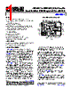
| Description | 700 MHz to 3000 MHz, Dual Passive Receive Mixer with Integrated PLL and VCO |







1. Overview & Context
️· Chip: ADRF6614
️· Type: This is a highly integrated RF chip likely used in a communications system (cellular, radio, etc.). The datasheet describes features related to frequency synthesis and signal generation, hinting at a potential role in an RF front-end.
️· Key Functions: Frequency generation, phase-locked loop (PLL) functionality, charge pump for voltage control, reference clocking, VCO control.
2. VCO (Voltage-Controlled Oscillator) and Phase Noise
️· Multiple VCOs: The chip features several VCOs: VCO_0, VCO_1, VCO_2, VCO_3, VCO_4, and VCO_5. Each VCO operates at a different frequency.
️· Phase Noise Performance: The datasheet includes extensive phase noise specifications for each VCO at various offset frequencies (1 kHz, 800 kHz, 1 MHz, 10 MHz, 40 MHz). Lower phase noise is *better* for signal quality.
- Example VCO_0 at 2.55 GHz: It boasts particularly good phase noise, with -87 dBc/Hz at 1 kHz offset.
️· RMS jitter: RMS jitter specs are provided for each VCO.
3. Charge Pump
️· Function: The charge pump is a critical part of the PLL feedback loop. It adjusts the voltage controlling the VCO.
️· Programmability: The pump current is programmable, allowing for fine-tuning of the PLL's response. The values range from 250 µA to 8 mA in steps of 500 µA.
4. Reference Characteristics
️· Reference Input: The chip requires a reference clock signal (REFIN).
️· Frequency Range: The reference input frequency range is 12 MHz to 320 MHz.
️· Divider: A programmable reference divider (0.5 to 2047) allows for a wide range of input frequencies.
️· MUXOUT: The MUXOUT signal provides level and duty cycle information.
5. Other Notable Specifications
️· Compliance Range: The charge pump's output compliance range is 0.7 V.
️· VCO Operating Frequencies: The VCO's operate at frequencies of 1.57 GHz to 2.55 GHz.
️· Input Capacitance: REFIN input capacitance is 4pF.
Overall Impression:
The ADRF6614 is a sophisticated RF chip designed for applications needing precise frequency generation and control. The datasheet highlights excellent VCO phase noise performance, programmability, and flexibility in reference clocking. Its complexity points to a likely role in a sophisticated RF system.
1. Overview & Context
️· Chip: ADRF6614
️· Type: This is a highly integrated RF chip likely used in a communications system (cellular, radio, etc.). The datasheet describes features related to frequency synthesis and signal generation, hinting at a potential role in an RF front-end.
️· Key Functions: Frequency generation, phase-locked loop (PLL) functionality, charge pump for voltage control, reference clocking, VCO control.
2. VCO (Voltage-Controlled Oscillator) and Phase Noise
️· Multiple VCOs: The chip features several VCOs: VCO_0, VCO_1, VCO_2, VCO_3, VCO_4, and VCO_5. Each VCO operates at a different frequency.
️· Phase Noise Performance: The datasheet includes extensive phase noise specifications for each VCO at various offset frequencies (1 kHz, 800 kHz, 1 MHz, 10 MHz, 40 MHz). Lower phase noise is *better* for signal quality.
- Example VCO_0 at 2.55 GHz: It boasts particularly good phase noise, with -87 dBc/Hz at 1 kHz offset.
️· RMS jitter: RMS jitter specs are provided for each VCO.
3. Charge Pump
️· Function: The charge pump is a critical part of the PLL feedback loop. It adjusts the voltage controlling the VCO.
️· Programmability: The pump current is programmable, allowing for fine-tuning of the PLL's response. The values range from 250 µA to 8 mA in steps of 500 µA.
4. Reference Characteristics
️· Reference Input: The chip requires a reference clock signal (REFIN).
️· Frequency Range: The reference input frequency range is 12 MHz to 320 MHz.
️· Divider: A programmable reference divider (0.5 to 2047) allows for a wide range of input frequencies.
️· MUXOUT: The MUXOUT signal provides level and duty cycle information.
5. Other Notable Specifications
️· Compliance Range: The charge pump's output compliance range is 0.7 V.
️· VCO Operating Frequencies: The VCO's operate at frequencies of 1.57 GHz to 2.55 GHz.
️· Input Capacitance: REFIN input capacitance is 4pF.
Overall Impression:
The ADRF6614 is a sophisticated RF chip designed for applications needing precise frequency generation and control. The datasheet highlights excellent VCO phase noise performance, programmability, and flexibility in reference clocking. Its complexity points to a likely role in a sophisticated RF system.
| Part No. | ADRF6614-EVALZ |
| Manufacturer | AD |
| Size | 2Mb |
| Pages | 61 pages |
| Description | 700 MHz to 3000 MHz, Dual Passive Receive Mixer with Integrated PLL and VCO |
| Czy Alldatasheet okazała się pomocna? [ DONATE ] |
O Alldatasheet | Reklama | Kontakt | Polityka prywatności | Link do karty katalogowej | Linki | Lista producentów All Rights Reserved©Alldatasheet.com |
| Russian : Alldatasheetru.com | Korean : Alldatasheet.co.kr | Spanish : Alldatasheet.es | French : Alldatasheet.fr | Italian : Alldatasheetit.com Portuguese : Alldatasheetpt.com | Polish : Alldatasheet.pl | Vietnamese : Alldatasheet.vn Indian : Alldatasheet.in | Mexican : Alldatasheet.com.mx | British : Alldatasheet.co.uk | New Zealand : Alldatasheet.co.nz |
|
Family Site : ic2ic.com |
icmetro.com |
 Polish ▼
  English
 Chinese
 German
 Japanese
 Russian
 Korean
 Spanish
 French
 Italian
 Portuguese
 Vietnamese
 Indian
 Mexican
 British
 New Zealand